Chips are the invisible foundation of the modern economy, but across Europe there are not enough people who can design and manufacture them. How can hands-on training – in laboratories and virtual environments – help, and what does this mean for Bulgaria?
The Invisible Foundation of Everyday Life
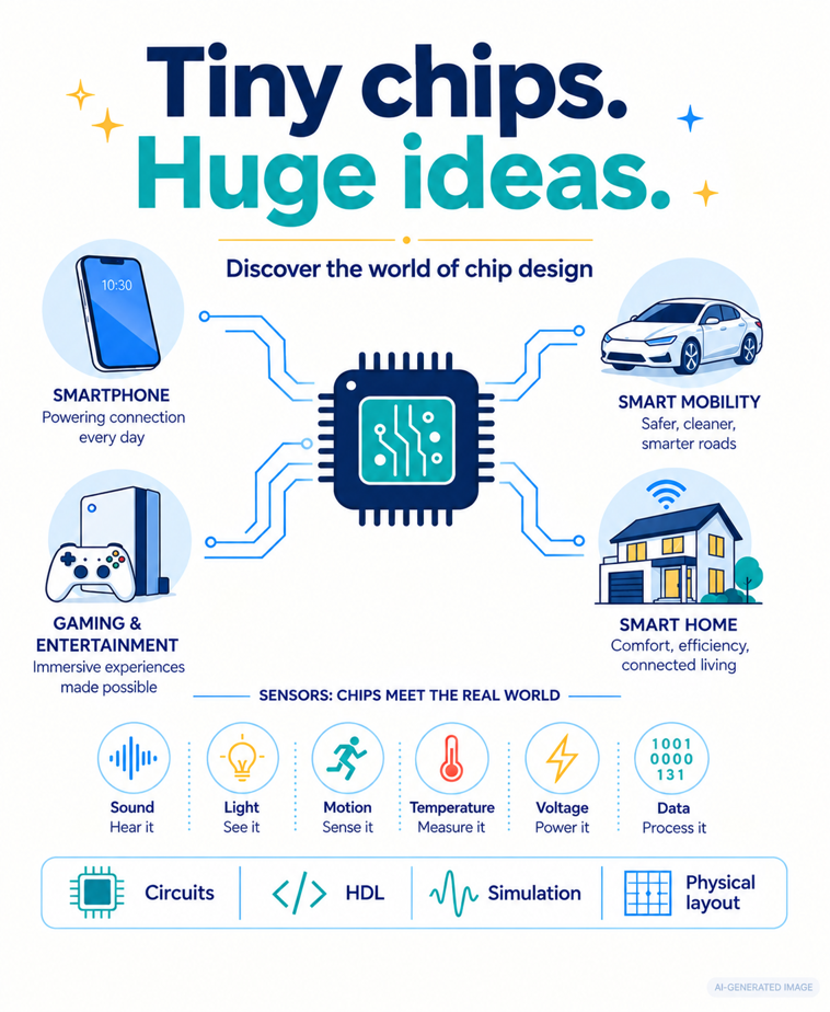
Chips are part of our everyday lives, although we are used to not noticing them. Modern phones cannot function without them, while cars have long ceased to be merely mechanical structures – their operation is based on electronics. Equipment in every sector – from medical diagnostics to production lines – operates with the help of chips. It is difficult to imagine healthcare, education, manufacturing of any kind, or even sport without the involvement of these small, invisible and almost miraculous components.
There is another dimension as well. Without chips, the development of artificial intelligence would not be possible – the language models that are talked about so much today run on specialized semiconductor devices. It is no coincidence that the European Commission defines semiconductors as the foundation of modern digital products and industries.
For this reason, the issue of chips has long been more than a technological one. It is a question of economic competitiveness, the resilience of supply chains, and Europe’s technological autonomy and even security. And behind every chip stands a long chain of people – designers, technologists, test engineers and technicians – who turn an idea into a working product.
Europe Has the Infrastructure, but Does It Have Enough People?
Europe is investing heavily in manufacturing capacity, research centers and design platforms. But infrastructure alone is not enough and does not create chips – people who know how to use it are needed. Manufacturing and integrating chips into different systems requires a new type of knowledge and skills, and Europe is paying serious attention to this sector, emphasizing that there is a significant shortage of engineers and technicians.
The problem is significant. Materials from the joint Chips JU initiative, dedicated to new calls for skills funding, state that according to the latest update of the European Skills Agenda, the sector faces a shortage of around 65,000 qualified specialists by 2030. The deficit affects the entire chain – from research and design to manufacturing and applications.
Technologies are developing so rapidly that training cannot be a one-time act. Programmes must continuously adapt to the next generation of technologies in order to meet new industry needs. In other words, lifelong learning is necessary, rather than one-off training – both for young people who are just entering the profession and for working engineers and technicians who need to build on or change their skills.
That is why experts recommend specialized training in different types of laboratories, where theory is inseparably linked to practice.
From “Learning About Chips” to “Learning by Working with Chips”
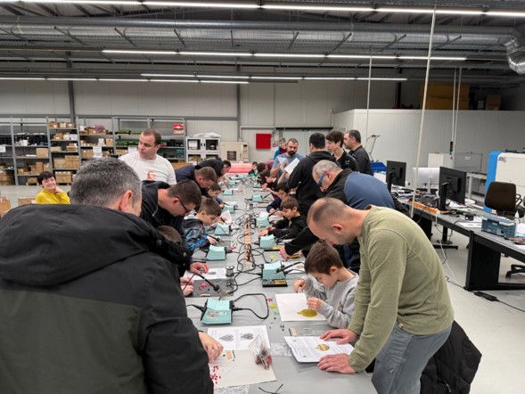
Learning by doing has long been a routine practice. Uno Cygnaeus introduced it in Finland under the name Sloyd. For example, a pupil or student first studies the principles of design, then creates a circuit, simulates it, tests it and prepares it for manufacturing. In this way, they are not only theoretically prepared for the process, but also have the opportunity to work in virtual laboratories and test their skills in practice – before ever setting foot in a real company. In Bulgaria, the Center for Research and Analysis partners with VekaTech and its STEMKids initiative to encourage pupils from an early age to experiment with chips, including designing them.
The same applies to rapidly developing technologies: alongside studying them, modern design tools can be used so that learners work with what industry itself uses. In this way, the approach shifts from “learning about chips” to “learning by working with chips” – from knowledge about chips to working with them.
What Makes a Programme Truly “Hands-On”
Not every training programme involving computers and simulations is practical in the sense we mean. A good chip-design programme usually combines several elements:
-
Working with real tools. Learners use the same class of software and workflows as engineers in industry, rather than simplified educational imitations.
-
A project from idea to finished design. Instead of isolated exercises, the student goes through the entire cycle – specification, design, simulation, verification and preparation for manufacturing.
-
Industry involvement. Real tasks, mentoring and lecturers from companies who show what is expected of a specialist in their first job.
-
Modularity. Short, stackable modules and micro-credentials that allow both students and working engineers to return to training throughout their professional careers.
Virtual Laboratories – Practice Without Cleanrooms
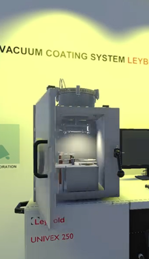
The main obstacle to practical training in microelectronics is cost. Cleanrooms and chip factories are extremely expensive, and no single university can afford to build and maintain them. That is why Europe is proposing virtual laboratories. Recently, they have become increasingly popular: quite often they are shared among different educational institutions and offer a set of modular training courses combined with practical sessions.
An example is the CHIPS of Europe project, funded under the Digital Europe Programme. Its virtual laboratory (VLabS) is designed so that students can gain practical experience in design, manufacturing and nanotechnology regardless of where they are located. According to its description on the European Digital Skills and Jobs Platform, the laboratory is hosted by FH Munich and is still under construction, but the first modules can already be tried out. In addition, the project develops micro-credentials, summer schools and training materials, while specifically working with high-school students and aiming to attract more women to the sector.
The advantages of such a model are several: accessibility (not every university has access to modern manufacturing facilities), lower cost, realistic scenarios close to work in industry, and a safe environment in which mistakes are part of learning rather than an expensive accident. A virtual laboratory does not fully replace physical practice, but it successfully fills the gap that would otherwise remain – the lack of costly physical infrastructure.
European design platforms are moving in the same direction. The EU Chips Design Platform brings together leading institutes from across Europe and provides access to design resources through a cloud-based virtual environment, while the Europractice 2.0 project aims to lower entry barriers for universities and research institutes by providing affordable, industry-standard design and training tools.
The Role of Universities and Competence Centers
Universities have a significant role in this approach. In the European discussion, there is frequent talk of “fourth-generation” universities: they not only teach knowledge, but also conduct research, play an important role for business and contribute to the development of the region in which they are located. Such universities host competence centers that bring together partner organizations from academia and business.
For the student, this means direct access to specialized companies and the opportunity to actively participate in parts of production chains, instead of their first encounter with industry taking place after graduation. This builds a network among universities, vocational schools and companies that supports the learning process from the school desk to the workplace.
Why Business Has an Interest in Hands-On Training?
Hands-on training is not solely the task of educational institutions – it is directly in companies’ interests as well. First, it shortens the time needed to reach the level of an independent specialist who can work with industrial tools, and this is among the expected outcomes of European skills centers of excellence – a shorter path from graduation to real work.
Second, companies gain access to talented pupils and students while they are still in training. They can participate in shaping curricula so that they reflect the real needs of industry.
Third, competence centers are also designed to support small and medium-sized enterprises – giving them access to pilot lines, the European design platform and training tailored to local and regional needs. For a country such as Bulgaria, where many technology companies are small, this is particularly important.
And What Is Being Done in Bulgaria?
To what extent can our universities offer practical training in microelectronics? A very good example is the Technical University of Sofia, which offers such training not only to students but also to pupils. The Technological School “Electronic Systems” (TUES) at the university is a specialized school with close ties to business, preparing excellent specialists, and its most successful graduates can continue directly at the university . Students, in turn, have direct access to the Center of Excellence in Mechatronics and Clean Technologies; the Competence Center for Intelligent Mechatronic, Eco- and Energy-Saving Systems and Technologies (IMEECT); as well as to the specialized laboratories of Sofia Tech Park.
These opportunities are complemented by the Competence Center in the field of integrated circuits, presented at the Technical University of Sofia in 2025 as part of the “Chips for Europe” initiative. It is designed as a driver of research, development and education in microelectronics – from chip design to support for high-tech start-ups. At the Technical University of Sofia there are various microelectronics laboratories, including NVIDIA’s high-tech center in partnership with ASBIS and Persy.
As an EU Member State, Bulgaria has access to European infrastructures and does not need to build such facilities independently. The virtual laboratory created through the CHIPS of Europe project provides excellent training opportunities and successfully fills the gap created by the lack of costly physical infrastructure, which is the most significant barrier for small and medium-sized universities.
Following the hands-on training approach, a TUES pupil takes their first steps in electronics and programming at school by participating in projects and competitions. As a student at the Technical University of Sofia, they work in a virtual laboratory and design their own project, and in the summer they intern at a company from the competence center’s partner network. When they graduate, they do not start with zero knowledge – they already know the tools, processes and people in the sector. This is the model toward which the hands-on approach strives: one continuous path instead of a series of separate and disconnected stages.
It is true that some of these elements in Bulgaria are still at an early stage of development, while others exist separately from one another. The challenge is not so much to create new structures as to connect those that already exist – schools, universities, laboratories, competence centers and companies – into a coherent system that is understandable to young people.
An Existing Deficit – Interest in Engineering Professions
A persistent problem is the insufficient number of students choosing engineering fields. This is partly an inertia dating back to the beginning of the transition, which is difficult to overcome, despite systematic efforts being made through regulation to address this deficit.
Here the hands-on approach has another role – not only to prepare learners, but also to attract them. A young person who has designed their own chip at the age of 17 sees the profession quite differently from someone who knows it only from a textbook. That is why early involvement of pupils and targeted efforts to attract girls and young people from diverse backgrounds are just as important as modernizing university programmes.
What Chips JU Is Offering in 2026
The European response to these challenges is becoming increasingly concrete. In 2026, the Chips JU initiative is offering separate skills strands, including Skills Hubs of Excellence, Pilot Federation and Stimulation of Chip Design. The calls opened on 7 July 2026, and the deadline for submitting proposals was 24 September 2026.
| Strand | Focus | Indicative budget |
|---|---|---|
| Skills Hubs of Excellence | Long-term centers for education, training, reskilling and talent attraction; close cooperation between academia and industry. | €20 million |
| Pilot Federation | Network of vocational education and training (VET) providers for practical training of technicians and reskilling of workers. | €10 million |
| Stimulation of Chip Design | Programme to inspire young people to pursue careers in the semiconductor sector – through student tape-out programmes and chip-design competitions. | €15 million |
Source: Chips JU; budgets are indicative.
The last strand – Stimulation of Chip Design – is particularly interesting. It is aimed specifically at attracting new generations to careers in the semiconductor sector through student tape-out programmes and chip design challenges. At least 60% of the budget must be directed to practical tape-out experience (through so-called multi-project wafers) for students and pupils, while one of the expected outcomes is for at least 1,000 students across Europe to complete funded tape-out projects over four years. In other words, European institutions are placing a direct bet on the hands-on approach – not only training people but also inspiring them.
Skills Hubs of Excellence are conceived as long-term centers that build on existing infrastructure – pilot lines, design platforms and competence centers. Pilot Federation, in turn, focuses on vocational education and training and on the shortage of technicians, aiming to connect existing European providers of such training in a common network.
For Bulgaria, this is a real opportunity. Universities, vocational schools, research institutes and companies in the country can join international consortia instead of relying solely on their own resources. Even for teams that did not participate in this round, the topics of the calls show the trends in European skills funding – and where it makes sense to invest already today.
In conclusion:
Europe has the ambition, manufacturing capacity and chip-design platforms. The next major competition, however, is for people – the engineers and technicians who will turn this infrastructure into real products. The answer is not more theory, but more practice: virtual and physical laboratories shared among institutions, close links between schools, universities and business, and learning that does not end with receiving a degree.
Bulgaria has both something to offer and something to benefit from – from TUES, the Technical University of Sofia, competence centers and a number of successful companies (for example EnduroSat) and start-ups, to European virtual laboratories and the new Chips JU programmes. The key question is whether we will manage to connect these elements into a functioning ecosystem and show young people that the path from the classroom to the chip is shorter than it initially appears.
picture 1
picture 2

picture 3
picture 4

picture 5
picture 6